Cadence OrCAD
New product
Software Cadence OrCAD Is a line of systems for the automated design of e
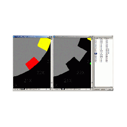
Software Cadence OrCAD Is a line of systems for the automated design of electronics (printed circuit boards and electronic circuits). The structure of the CAD package OrCAD Includes solutions for editing schematic diagrams, managing Active Parts libraries, analog-digital modeling, parametric optimization, interaction with the MATLAB environment, editing PCB topologies, automatic and interactive tracing, signal integrity analysis and cross-distortion. To the new version OrCAD 16.6 Added features and approaches to the design of printed circuit boards and the modeling of electronic circuits. A key feature of OrCAD 16.6 is the implementation of a new design flow with the inclusion of signal integrity analysis at the circuit level. This flow provides a higher level of automation when modeling high-speed digital circuits. Components of Cadence OrCAD:
OrCAD PSpice AD and Advanced Analysis Modeling with PSpice is a fast, simple and reliable way of performing circuit calculations. With the help of OrCAD PSpice, it is possible to create schemes where the scatter of the parameters of the elements is maximally optimized, taking into account their tolerances, which will not be too stringent (this will not provoke a rise in price) and free enough (this will not increase the reject rate). This leads to an increase in the profitability of production, a reduction in the prototyping stage, a reduction in the time spent on laboratory research and, ultimately, a decrease in the cost of production and an increase in its competitiveness in the market.
PSpice technologies are advanced, popular in the production of analog, digital and mixed analog-digital modeling tools for electrical engineers. Using PSpice, it is possible to model a wide range of circuits - from power supplies to high-frequency systems and small chips. OrCAD PCB Editor CadenceOrCAD PCB Editor is a part of the OrCAD PCB Designer software package and provides extensive possibilities for designing the topology of printed circuit boards. In combination with an intuitive interface and a large set of rules for specifying design constraints, PCB Editor allows you to solve numerous tasks faced by PCB design engineers, including improving the process design. OrCAD Signal Explorer Cadence OrCAD Signal Explorer is a module for pre- and post-analysis analysis of signal integrity, combining the benefits of interaction between the design and modeling environment. The Signal Explorer product is closely associated with the OrCAD PCB Editor. Signal Explorer is a scalable solution that significantly reduces the cost of developing a printed circuit board. If the level of development grows, the Signal Explorer can easily update the Cadence Allegro PCB SI solution. The Signal Explorer module can significantly speed up the work of engineers in designing high-density boards, and also reduce the likelihood of errors. OrCAD FPGA System Planner The solution for integrated projects "PCB - FPGA" with two-way information exchange and automatic tracking of information change in FPGA and on PCB. The product implements the function of loading the arrangement of FPGA outputs, generation of symbols and their addition to the circuit design of the printed circuit board. Cadence FPGA System Planner Is a powerful tool for creating projects based on FPGA, which includes all the necessary tools for assigning and optimizing outputs, providing high traceability of devices using FPGAs on printed circuit boards. FPGA System Planner Significantly reduces the debugging time of complex projects with several multi-output FPGAs through end-to-end system-level design, automatic routing and link optimization, and reliable protection from manual design errors. Significantly reduces the debugging time of complex projects with several multi-output FPGAs through end-to-end system-level design, automatic routing and link optimization, and reliable protection from manual design errors. Significantly reduces the debugging time of complex projects with several multi-output FPGAs through end-to-end system-level design, automatic routing and link optimization, and reliable protection from manual design errors. Significantly reduces the debugging time of complex projects with several multi-output FPGAs through end-to-end system-level design, automatic routing and link optimization, and reliable protection from manual design errors. Significantly reduces the debugging time of complex projects with several multi-output FPGAs through end-to-end system-level design, automatic routing and link optimization, and reliable protection from manual design errors. Significantly reduces the debugging time of complex projects with several multi-output FPGAs through end-to-end system-level design, automatic routing and link optimization, and reliable protection from manual design errors.
- Capture is a graphical schematic editor.
- Capture CIS is a graphical schematic editor with a component database management tool.
- PSpice A / D is a program for simulating analog and mixed analog-to-digital devices, the data is transferred to both from PSpice Schematics and from OrCAD Capture.
- PSpice AA is a solution for parametric optimization.
- PSpice SLPS Option is a communication module with the MATLAB package.
- SPECCTRA - program for automatic trace of printed circuit boards from the Cadence OrCAD package.
- PCB Editor - a system for editing the topology of printed circuit boards.
- Signal Explorer is an application for analyzing the integrity of the signal and the interference of components in the board.
OrCAD PSpice AD and Advanced Analysis Modeling with PSpice is a fast, simple and reliable way of performing circuit calculations. With the help of OrCAD PSpice, it is possible to create schemes where the scatter of the parameters of the elements is maximally optimized, taking into account their tolerances, which will not be too stringent (this will not provoke a rise in price) and free enough (this will not increase the reject rate). This leads to an increase in the profitability of production, a reduction in the prototyping stage, a reduction in the time spent on laboratory research and, ultimately, a decrease in the cost of production and an increase in its competitiveness in the market.
PSpice technologies are advanced, popular in the production of analog, digital and mixed analog-digital modeling tools for electrical engineers. Using PSpice, it is possible to model a wide range of circuits - from power supplies to high-frequency systems and small chips. OrCAD PCB Editor CadenceOrCAD PCB Editor is a part of the OrCAD PCB Designer software package and provides extensive possibilities for designing the topology of printed circuit boards. In combination with an intuitive interface and a large set of rules for specifying design constraints, PCB Editor allows you to solve numerous tasks faced by PCB design engineers, including improving the process design. OrCAD Signal Explorer Cadence OrCAD Signal Explorer is a module for pre- and post-analysis analysis of signal integrity, combining the benefits of interaction between the design and modeling environment. The Signal Explorer product is closely associated with the OrCAD PCB Editor. Signal Explorer is a scalable solution that significantly reduces the cost of developing a printed circuit board. If the level of development grows, the Signal Explorer can easily update the Cadence Allegro PCB SI solution. The Signal Explorer module can significantly speed up the work of engineers in designing high-density boards, and also reduce the likelihood of errors. OrCAD FPGA System Planner The solution for integrated projects "PCB - FPGA" with two-way information exchange and automatic tracking of information change in FPGA and on PCB. The product implements the function of loading the arrangement of FPGA outputs, generation of symbols and their addition to the circuit design of the printed circuit board. Cadence FPGA System Planner Is a powerful tool for creating projects based on FPGA, which includes all the necessary tools for assigning and optimizing outputs, providing high traceability of devices using FPGAs on printed circuit boards. FPGA System Planner Significantly reduces the debugging time of complex projects with several multi-output FPGAs through end-to-end system-level design, automatic routing and link optimization, and reliable protection from manual design errors. Significantly reduces the debugging time of complex projects with several multi-output FPGAs through end-to-end system-level design, automatic routing and link optimization, and reliable protection from manual design errors. Significantly reduces the debugging time of complex projects with several multi-output FPGAs through end-to-end system-level design, automatic routing and link optimization, and reliable protection from manual design errors. Significantly reduces the debugging time of complex projects with several multi-output FPGAs through end-to-end system-level design, automatic routing and link optimization, and reliable protection from manual design errors. Significantly reduces the debugging time of complex projects with several multi-output FPGAs through end-to-end system-level design, automatic routing and link optimization, and reliable protection from manual design errors. Significantly reduces the debugging time of complex projects with several multi-output FPGAs through end-to-end system-level design, automatic routing and link optimization, and reliable protection from manual design errors.
Related Products


.jpg)

.jpg)
.jpg)
.jpg)
.jpg)
.jpg)


.jpg)


.jpg)
.jpg)
.jpg)